
TSMC Beol Memory Reached! 0.017 μm ² Cell Area Rigid 3D DRAM
Fast Technology reported on November 9 that TSMC's recent actions in the storage field have shown obvious duality. On the one hand, the company publicly denied that it had developed 3D DRAM at the request of Nvidia, emphasizing its focus on the core business of foundry. On the other hand, its BEOL (post-process) memory technology has entered the experimental stage, and the goal is to solve the problem of the capacity and power consumption of the embedded cache on the logic chip.
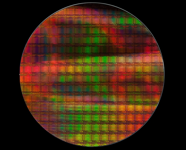
The core innovation of BEOL memory is structure. Traditional SRAM cells require 6 transistors and occupy a large area on the chip. TSMC switched to a 1T1C (single transistor single capacitor) architecture, embedding the memory cells directly into the rear interconnect layer of the processor, and plugging in more data without increasing the chip area.
The parameter indicators are quite clear. The operating voltage of this experimental sample is only 0.75 V, the data retention time exceeds 128 milliseconds, the read/write cycle is less than 8 nanoseconds, and the durability exceeds 100 trillion cycles.
More critically, the SRAM cell area of TSMC's A14 node has been reduced to less than 0.017 square microns, which is about 19% smaller than before, breaking an eight-year stagnation.
But this is not the same as 3D DRAM. Beol memory solves the problem of "not large enough cache" inside the logic chip, while 3D DRAM solves the problem of "not enough memory". The former is an alternative to SRAM and the latter is a vertical stacking route for DRAM. The two advance in parallel in TSMC's layout, but at different rhythms.
TSMC's 3D DRAM roadmap anchors 2029 with the goal of achieving approximately 3 times the bandwidth of HBM5E at less than 1 picajoule per bit of energy consumption. The program is led by Xu Guojin, a deputy general manager in charge of advanced packaging business, who previously served as the chairman of Micron in Taiwan, China, and has a background in storage manufacturing and chip integration.
Therefore, TSMC's "denial" needs to be understood hierarchically. It denies large-scale entry into DRAM manufacturing in the short term, competing head-to-head with Samsung and Hynix, but does not deny the long-term technology reserve on Beol memory and 3D DRAM.
When the BEOL memory greatly increases the cache capacity of the logic chip itself, 3D DRAM allows the memory cells to stack in the vertical direction. The superimposed effect of the two is that the dependence of the AI chip on HBM is structurally weakened.
Nvidia's anxiety is the catalyst for this change. HBM supply is highly concentrated in Samsung, SK Hynix and Micron, and prices and production capacity are subject to people. The essence of TSMC's Beol memory and 3D DRAM is to find a memory supply path for AI chips that does not rely on traditional storage giants.
Whether this path can be followed around 2029 will determine whether the memory layout of AI chips needs to be rewritten.
Source: MyDrivers (Fast Technology). Content is presented with source attribution. Read the original report.
Back to News